Beginners Setup Guide Renard Boards with External SSR: Difference between revisions
| (8 intermediate revisions by one other user not shown) | |||
| Line 11: | Line 11: | ||
! <center>'''Multimeter Usage Tip'''</center> | ! <center>'''Multimeter Usage Tip'''</center> | ||
|- | |- | ||
| All DC voltages in this document are referenced to GND. So for all measurements, the multimeter negative (-), usually black, lead needs to be connected to a GND point on the PCB. The best location would be the GND Test Point located | | All ''DC voltages'' in this document are referenced to GND. So for all measurements, the multimeter negative (-), usually black, lead needs to be connected to a GND point on the PCB. The best location would be TP1 which is the GND Test Point located near J21. The positive lead (+), usually red, gets connected to the location called out in the procedure. | ||
|} | |} | ||
| Line 25: | Line 25: | ||
<li>Remove all cables | <li>Remove all cables | ||
<li>If installed, remove all the removable IC chips. For this example, the REN64 will be used. For other boards, the items will be similar but the chip number may be different. | <li>If installed, remove all the removable IC chips. For this example, the REN64 will be used. For other boards, the items will be similar but the chip number may be different. The REN64XC chips to be removed are: U3, U4, U5, U7-U14. | ||
<li>Perform a complete and thorough inspection of the underside of the PCB. | <li>Perform a complete and thorough inspection of the underside of the PCB. | ||
| Line 32: | Line 32: | ||
:* Make sure the board surface is clean and free from any debris and flux residue. | :* Make sure the board surface is clean and free from any debris and flux residue. | ||
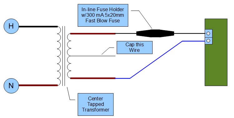
<li>Connect a 6.3VAC power supply to Tab1/Tab2. This requires understanding how to wire up the transformer. | <li>Connect a 6.3VAC power supply to Tab1/Tab2. This requires understanding how to wire up the transformer. If you are using this guide, it is suggested that you install an inline fuse for troubleshooting purposes. | ||
[[Image: Transfomer.png|center]] | |||
<li>Turn ON AC power | <li>Turn ON AC power | ||
<li>Measure DC voltage at the | <li>Measure DC voltage at U1. This is the lead closest to U4. You can also measure this at the input to R8 next to U5. | ||
:*It should be 5.0 (+/- .1) VDC. | :*It should be 5.0 (+/- .1) VDC. | ||
:*If incorrect , then go to the [[ | :*If incorrect , then go to the [[Troubleshooting_Guide_Renard_64XC#Troubleshooting_Power_Problems | Renard 64XC Troubleshooting Guide]]. | ||
<li>Power LED should be lit. | <li>Power LED should be lit. | ||
:*If it didn’t , then go to the [[ | :*If it didn’t , then go to the [[Troubleshooting_Guide_Renard_64XC#Troubleshooting_Power_Problems | Renard 64XC Troubleshooting Guide]]. | ||
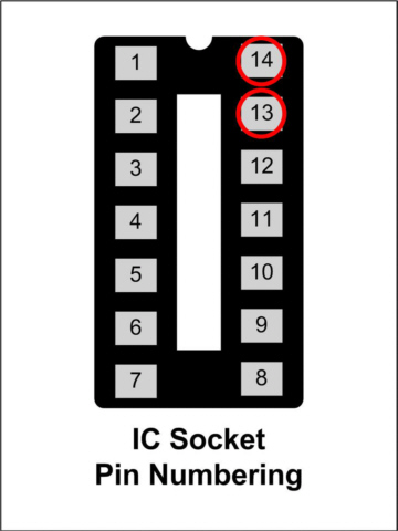
<li>Momentarily connect a jumper (small piece of wire) between | <li>Momentarily connect a jumper (small piece of wire) between U10 [[media: Wiki - IC socket 13-14.jpg | IC socket pin 13 and pin 14]]. | ||
:*Channel | :*Channel 2 LED should light-->This is the HB LED. Once again, the chip numbering is specific to the Renard 64XC. Some Renard boards have specific LEDs for the HB or "Heart Beat" Function. | ||
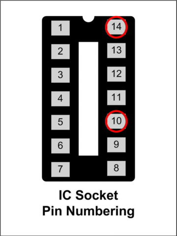
<li>Momentarily connect a jumper between | <li>Momentarily connect a jumper between U10 [[media: Wiki - IC socket 10-14.jpg | IC socket pin 10 and pin 14]] | ||
:*Channel | :*Channel 5 LED should light -->This is the ZC or "Zero Crossing" LED. | ||
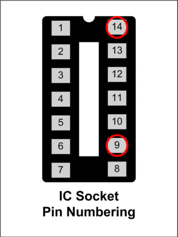
<li>Momentarily connect a jumper between | <li>Momentarily connect a jumper between U10 [[media: Wiki - IC socket 9-14.jpg | IC socket pin 9 and pin 14]] | ||
:*Channel | :*Channel 6 LED should light -->This is the SD or "Data" LED. | ||
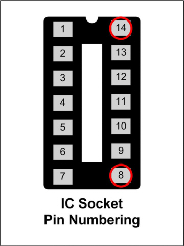
<li>Momentarily connect a jumper between | <li>Momentarily connect a jumper between U10 [[media: Wiki - IC socket 8-14.jpg | IC socket pin 8 and pin 14]] | ||
:*Channel | :*Channel 7 LED should light -->This is the FE or "Framing Error" LED. | ||
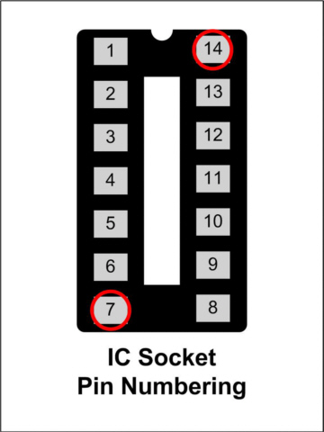
<li>Momentarily connect a jumper between | <li>Momentarily connect a jumper between U10 [[media: Wiki - IC socket 7-14.jpg | IC socket pin 7 and pin 14]] | ||
:*Channel | :*Channel 8 LED should light -->This is the OE or "Overun" LED. | ||
<li>If any of the LEDs in steps 11 thru 15 did not light, then go to the [[ | <li>If any of the LEDs in steps 11 thru 15 did not light, then go to the [[Troubleshooting_Guide_Renard_64XC#Verifying_Diagnostic_LEDs | Renard 64XC Troubleshooting Guide]]. | ||
<li>Turn OFF AC power. | <li>Turn OFF AC power. | ||
<li>Install a SSR like the SSRez into | <li>Install a SSR like the SSRez into J12 with a known good straight through CAT5 cable. If you are not sure that the cable is good, use the DMM to ring out the cable. | ||
<li>Attach some test lights to the SSR terminal block for Channel 1. | <li>Attach some test lights to the SSR terminal block for Channel 1. | ||
| Line 72: | Line 74: | ||
<li>Test lights should be OFF. | <li>Test lights should be OFF. | ||
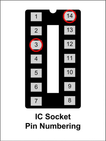
<li>Momentarily connect a jumper (small piece of wire) between | <li>Momentarily connect a jumper (small piece of wire) between U10 [[media: Wiki - IC socket 3-14.jpg | IC socket pin 3 and pin 14]]. | ||
:*Test lights should come ON when the jumper is connected. | :*Test lights should come ON when the jumper is connected. | ||
<li>If either step 23 or step 24 failed, then go to the [[ | <li>If either step 23 or step 24 failed, then go to the [[Troubleshooting_Guide_Renard_64XC#Troubleshooting_SSR_Circuitry_Problems | Renard 64XC Troubleshooting Guide]]. | ||
<li>Repeat steps 18 thru 25 using the information in the table. Once again, the IC Chip numbering | <li>Repeat steps 18 thru 25 using the information in the table. Once again, the IC Chip numbering and the Jack numbering are for the Renard 64XC. | ||
<br> | <br> | ||
| Line 87: | Line 89: | ||
!width="250"| Connect jumper between | !width="250"| Connect jumper between | ||
|- | |- | ||
|Channel 1|| | |Channel 1||U10|| J12 || Channel 1 | ||
|align="left"| | |align="left"| | ||
:[[media: Wiki - IC socket 3-14.jpg | IC Socket Pin 3 -> Pin 14]] | :[[media: Wiki - IC socket 3-14.jpg | IC Socket Pin 3 -> Pin 14]] | ||
|- | |- | ||
|Channel 2|| | |Channel 2||U10|| J12 || Channel 2 | ||
|align="left"| | |align="left"| | ||
:[[media: Wiki - IC socket 13-14.jpg | IC Socket Pin 13 -> Pin 14]] | :[[media: Wiki - IC socket 13-14.jpg | IC Socket Pin 13 -> Pin 14]] | ||
|- | |- | ||
|Channel 3|| | |Channel 3||U10|| J12 || Channel 3 | ||
|align="left"| | |align="left"| | ||
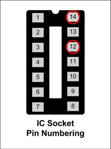
:[[media: Wiki - IC socket 12-14.jpg | IC Socket Pin 12 -> Pin 14]] | :[[media: Wiki - IC socket 12-14.jpg | IC Socket Pin 12 -> Pin 14]] | ||
|- | |- | ||
|Channel 4|| | |Channel 4||U10|| J12 || Channel 4 | ||
|align="left"| | |align="left"| | ||
:[[media: Wiki - IC socket 11-14.jpg | IC Socket Pin 11 -> Pin 14]] | :[[media: Wiki - IC socket 11-14.jpg | IC Socket Pin 11 -> Pin 14]] | ||
|- | |- | ||
|Channel 5|| | |Channel 5||U10|| J8 || Channel 1 | ||
|align="left"| | |align="left"| | ||
:[[media: Wiki - IC socket 10-14.jpg | IC Socket Pin 10 -> Pin 14]] | :[[media: Wiki - IC socket 10-14.jpg | IC Socket Pin 10 -> Pin 14]] | ||
|- | |- | ||
|Channel 6|| | |Channel 6||U10|| J8 || Channel 2 | ||
|align="left"| | |align="left"| | ||
:[[media: Wiki - IC socket 9-14.jpg | IC Socket Pin 9 and -> Pin 14]] | :[[media: Wiki - IC socket 9-14.jpg | IC Socket Pin 9 and -> Pin 14]] | ||
|- | |- | ||
|Channel 7|| | |Channel 7||U10|| J8 || Channel 3 | ||
|align="left"| | |align="left"| | ||
:[[media: Wiki - IC socket 8-14.jpg | IC Socket Pin 8 and -> Pin 14]] | :[[media: Wiki - IC socket 8-14.jpg | IC Socket Pin 8 and -> Pin 14]] | ||
|- | |- | ||
|Channel 8|| | |Channel 8||U10|| J8 || Channel 4 | ||
|align="left"| | |align="left"| | ||
:[[media: Wiki - IC socket 7-14.jpg | IC Socket Pin 7 and -> Pin 14]] | :[[media: Wiki - IC socket 7-14.jpg | IC Socket Pin 7 and -> Pin 14]] | ||
|- | |- | ||
|Channel 9|| | |Channel 9||U9|| J11 || Channel 1 | ||
|align="left"| | |align="left"| | ||
:[[media: Wiki - IC socket 3-14.jpg | IC Socket Pin 3 -> Pin 14]] | :[[media: Wiki - IC socket 3-14.jpg | IC Socket Pin 3 -> Pin 14]] | ||
|- | |- | ||
|Channel 10|| | |Channel 10||U9|| J11 || Channel 2 | ||
|align="left"| | |align="left"| | ||
:[[media: Wiki - IC socket 13-14.jpg | IC Socket Pin 13 -> Pin 14]] | :[[media: Wiki - IC socket 13-14.jpg | IC Socket Pin 13 -> Pin 14]] | ||
|- | |- | ||
|Channel 11|| | |Channel 11||U9|| J11 || Channel 3 | ||
|align="left"| | |align="left"| | ||
:[[media: Wiki - IC socket 12-14.jpg | IC Socket Pin 12 -> Pin 14]] | :[[media: Wiki - IC socket 12-14.jpg | IC Socket Pin 12 -> Pin 14]] | ||
|- | |- | ||
|Channel 12|| | |Channel 12||U9|| J11 || Channel 4 | ||
|align="left"| | |align="left"| | ||
:[[media: Wiki - IC socket 11-14.jpg | IC Socket Pin 11 -> Pin 14]] | :[[media: Wiki - IC socket 11-14.jpg | IC Socket Pin 11 -> Pin 14]] | ||
|- | |- | ||
|Channel 13|| | |Channel 13||U9|| J7 || Channel 1 | ||
|align="left"| | |align="left"| | ||
:[[media: Wiki - IC socket 10-14.jpg | IC Socket Pin 10 -> Pin 14]] | :[[media: Wiki - IC socket 10-14.jpg | IC Socket Pin 10 -> Pin 14]] | ||
|- | |- | ||
|Channel 14|| | |Channel 14||U9|| J7 || Channel 2 | ||
|align="left"| | |align="left"| | ||
:[[media: Wiki - IC socket 9-14.jpg | IC Socket Pin 9 and -> Pin 14]] | :[[media: Wiki - IC socket 9-14.jpg | IC Socket Pin 9 and -> Pin 14]] | ||
|- | |- | ||
|Channel 15|| | |Channel 15||U9|| J7 || Channel 3 | ||
|align="left"| | |align="left"| | ||
:[[media: Wiki - IC socket 8-14.jpg | IC Socket Pin 8 and -> Pin 14]] | :[[media: Wiki - IC socket 8-14.jpg | IC Socket Pin 8 and -> Pin 14]] | ||
|- | |- | ||
|Channel 16|| | |Channel 16||U9|| J7 || Channel 4 | ||
|align="left"| | |align="left"| | ||
:[[media: Wiki - IC socket 7-14.jpg | IC Socket Pin 7 and -> Pin 14]] | :[[media: Wiki - IC socket 7-14.jpg | IC Socket Pin 7 and -> Pin 14]] | ||
|- | |- | ||
|Channel 17|| | |Channel 17||U8|| J10 || Channel 1 | ||
|align="left"| | |align="left"| | ||
:[[media: Wiki - IC socket 3-14.jpg | IC Socket Pin 3 -> Pin 14]] | :[[media: Wiki - IC socket 3-14.jpg | IC Socket Pin 3 -> Pin 14]] | ||
|- | |- | ||
|Channel 18|| | |Channel 18||U8|| J10 || Channel 2 | ||
|align="left"| | |align="left"| | ||
:[[media: Wiki - IC socket 13-14.jpg | IC Socket Pin 13 -> Pin 14]] | :[[media: Wiki - IC socket 13-14.jpg | IC Socket Pin 13 -> Pin 14]] | ||
|- | |- | ||
|Channel 19|| | |Channel 19||U8|| J10 || Channel 3 | ||
|align="left"| | |align="left"| | ||
:[[media: Wiki - IC socket 12-14.jpg | IC Socket Pin 12 -> Pin 14]] | :[[media: Wiki - IC socket 12-14.jpg | IC Socket Pin 12 -> Pin 14]] | ||
|- | |- | ||
|Channel 20|| | |Channel 20||U8|| J10 || Channel 4 | ||
|align="left"| | |align="left"| | ||
:[[media: Wiki - IC socket 11-14.jpg | IC Socket Pin 11 -> Pin 14]] | :[[media: Wiki - IC socket 11-14.jpg | IC Socket Pin 11 -> Pin 14]] | ||
|- | |- | ||
|Channel 21|| | |Channel 21||U8|| J6 || Channel 1 | ||
|align="left"| | |align="left"| | ||
:[[media: Wiki - IC socket 10-14.jpg | IC Socket Pin 10 -> Pin 14]] | :[[media: Wiki - IC socket 10-14.jpg | IC Socket Pin 10 -> Pin 14]] | ||
|- | |- | ||
|Channel 22|| | |Channel 22||U8|| J6 || Channel 2 | ||
|align="left"| | |align="left"| | ||
:[[media: Wiki - IC socket 9-14.jpg | IC Socket Pin 9 and -> Pin 14]] | :[[media: Wiki - IC socket 9-14.jpg | IC Socket Pin 9 and -> Pin 14]] | ||
|- | |- | ||
|Channel 23|| | |Channel 23||U8|| J6 || Channel 3 | ||
|align="left"| | |align="left"| | ||
:[[media: Wiki - IC socket 8-14.jpg | IC Socket Pin 8 and -> Pin 14]] | :[[media: Wiki - IC socket 8-14.jpg | IC Socket Pin 8 and -> Pin 14]] | ||
|- | |- | ||
|Channel 24|| | |Channel 24||U8|| J6 || Channel 4 | ||
|align="left"| | |align="left"| | ||
:[[media: Wiki - IC socket 7-14.jpg | IC Socket Pin 7 and -> Pin 14]] | :[[media: Wiki - IC socket 7-14.jpg | IC Socket Pin 7 and -> Pin 14]] | ||
|- | |- | ||
|Channel 25|| | |Channel 25||U7|| J9 || Channel 1 | ||
|align="left"| | |align="left"| | ||
:[[media: Wiki - IC socket 3-14.jpg | IC Socket Pin 3 -> Pin 14]] | :[[media: Wiki - IC socket 3-14.jpg | IC Socket Pin 3 -> Pin 14]] | ||
|- | |- | ||
|Channel 26|| | |Channel 26||U7|| J9 || Channel 2 | ||
|align="left"| | |align="left"| | ||
:[[media: Wiki - IC socket 13-14.jpg | IC Socket Pin 13 -> Pin 14]] | :[[media: Wiki - IC socket 13-14.jpg | IC Socket Pin 13 -> Pin 14]] | ||
|- | |- | ||
|Channel 27|| | |Channel 27||U7|| J9 || Channel 3 | ||
|align="left"| | |align="left"| | ||
:[[media: Wiki - IC socket 12-14.jpg | IC Socket Pin 12 -> Pin 14]] | :[[media: Wiki - IC socket 12-14.jpg | IC Socket Pin 12 -> Pin 14]] | ||
|- | |- | ||
|Channel 28|| | |Channel 28||U7|| J9 || Channel 4 | ||
|align="left"| | |align="left"| | ||
:[[media: Wiki - IC socket 11-14.jpg | IC Socket Pin 11 -> Pin 14]] | :[[media: Wiki - IC socket 11-14.jpg | IC Socket Pin 11 -> Pin 14]] | ||
|- | |- | ||
|Channel 29|| | |Channel 29||U7|| J5 || Channel 1 | ||
|align="left"| | |align="left"| | ||
:[[media: Wiki - IC socket 10-14.jpg | IC Socket Pin 10 -> Pin 14]] | :[[media: Wiki - IC socket 10-14.jpg | IC Socket Pin 10 -> Pin 14]] | ||
|- | |- | ||
|Channel 30|| | |Channel 30||U7|| J5 || Channel 2 | ||
|align="left"| | |align="left"| | ||
:[[media: Wiki - IC socket 9-14.jpg | IC Socket Pin 9 and -> Pin 14]] | :[[media: Wiki - IC socket 9-14.jpg | IC Socket Pin 9 and -> Pin 14]] | ||
|- | |- | ||
|Channel 31|| | |Channel 31||U7|| J5 || Channel 3 | ||
|align="left"| | |align="left"| | ||
:[[media: Wiki - IC socket 8-14.jpg | IC Socket Pin 8 and -> Pin 14]] | :[[media: Wiki - IC socket 8-14.jpg | IC Socket Pin 8 and -> Pin 14]] | ||
|- | |- | ||
|Channel 32|| | |Channel 32||U7|| J5 || Channel 4 | ||
|align="left"| | |align="left"| | ||
:[[media: Wiki - IC socket 7-14.jpg | IC Socket Pin 7 and -> Pin 14]] | :[[media: Wiki - IC socket 7-14.jpg | IC Socket Pin 7 and -> Pin 14]] | ||
|- | |- | ||
|Channel 33|| | |Channel 33||U14|| J21 || Channel 1 | ||
|align="left"| | |align="left"| | ||
:[[media: Wiki - IC socket 3-14.jpg | IC Socket Pin 3 -> Pin 14]] | :[[media: Wiki - IC socket 3-14.jpg | IC Socket Pin 3 -> Pin 14]] | ||
|- | |- | ||
|Channel 34|| | |Channel 34||U14|| J21 || Channel 2 | ||
|align="left"| | |align="left"| | ||
:[[media: Wiki - IC socket 13-14.jpg | IC Socket Pin 13 -> Pin 14]] | :[[media: Wiki - IC socket 13-14.jpg | IC Socket Pin 13 -> Pin 14]] | ||
|- | |- | ||
|Channel 35|| | |Channel 35||U14|| J21 || Channel 3 | ||
|align="left"| | |align="left"| | ||
:[[media: Wiki - IC socket 12-14.jpg | IC Socket Pin 12 -> Pin 14]] | :[[media: Wiki - IC socket 12-14.jpg | IC Socket Pin 12 -> Pin 14]] | ||
|- | |- | ||
|Channel 36|| | |Channel 36||U14|| J21 || Channel 4 | ||
|align="left"| | |align="left"| | ||
:[[media: Wiki - IC socket 11-14.jpg | IC Socket Pin 11 -> Pin 14]] | :[[media: Wiki - IC socket 11-14.jpg | IC Socket Pin 11 -> Pin 14]] | ||
|- | |- | ||
|Channel 37|| | |Channel 37||U14|| J16 || Channel 1 | ||
|align="left"| | |align="left"| | ||
:[[media: Wiki - IC socket 10-14.jpg | IC Socket Pin 10 -> Pin 14]] | :[[media: Wiki - IC socket 10-14.jpg | IC Socket Pin 10 -> Pin 14]] | ||
|- | |- | ||
|Channel 38|| | |Channel 38||U14|| J16 || Channel 2 | ||
|align="left"| | |align="left"| | ||
:[[media: Wiki - IC socket 9-14.jpg | IC Socket Pin 9 and -> Pin 14]] | :[[media: Wiki - IC socket 9-14.jpg | IC Socket Pin 9 and -> Pin 14]] | ||
|- | |- | ||
|Channel 39|| | |Channel 39||U14|| J16 || Channel 3 | ||
|align="left"| | |align="left"| | ||
:[[media: Wiki - IC socket 8-14.jpg | IC Socket Pin 8 and -> Pin 14]] | :[[media: Wiki - IC socket 8-14.jpg | IC Socket Pin 8 and -> Pin 14]] | ||
|- | |- | ||
|Channel 40|| | |Channel 40||U14|| J16 || Channel 4 | ||
|align="left"| | |align="left"| | ||
:[[media: Wiki - IC socket 7-14.jpg | IC Socket Pin 7 and -> Pin 14]] | :[[media: Wiki - IC socket 7-14.jpg | IC Socket Pin 7 and -> Pin 14]] | ||
|- | |- | ||
|Channel 41|| | |Channel 41||U13|| J20 || Channel 1 | ||
|align="left"| | |align="left"| | ||
:[[media: Wiki - IC socket 3-14.jpg | IC Socket Pin 3 -> Pin 14]] | :[[media: Wiki - IC socket 3-14.jpg | IC Socket Pin 3 -> Pin 14]] | ||
|- | |- | ||
|Channel 42|| | |Channel 42||U13|| J20 || Channel 2 | ||
|align="left"| | |align="left"| | ||
:[[media: Wiki - IC socket 13-14.jpg | IC Socket Pin 13 -> Pin 14]] | :[[media: Wiki - IC socket 13-14.jpg | IC Socket Pin 13 -> Pin 14]] | ||
|- | |- | ||
|Channel 43|| | |Channel 43||U13|| J20 || Channel 3 | ||
|align="left"| | |align="left"| | ||
:[[media: Wiki - IC socket 12-14.jpg | IC Socket Pin 12 -> Pin 14]] | :[[media: Wiki - IC socket 12-14.jpg | IC Socket Pin 12 -> Pin 14]] | ||
|- | |- | ||
|Channel 44|| | |Channel 44||U13|| J20 || Channel 4 | ||
|align="left"| | |align="left"| | ||
:[[media: Wiki - IC socket 11-14.jpg | IC Socket Pin 11 -> Pin 14]] | :[[media: Wiki - IC socket 11-14.jpg | IC Socket Pin 11 -> Pin 14]] | ||
|- | |- | ||
|Channel 45|| | |Channel 45||U13|| J15 || Channel 1 | ||
|align="left"| | |align="left"| | ||
:[[media: Wiki - IC socket 10-14.jpg | IC Socket Pin 10 -> Pin 14]] | :[[media: Wiki - IC socket 10-14.jpg | IC Socket Pin 10 -> Pin 14]] | ||
|- | |- | ||
|Channel 46|| | |Channel 46||U13|| J15 || Channel 2 | ||
|align="left"| | |align="left"| | ||
:[[media: Wiki - IC socket 9-14.jpg | IC Socket Pin 9 and -> Pin 14]] | :[[media: Wiki - IC socket 9-14.jpg | IC Socket Pin 9 and -> Pin 14]] | ||
|- | |- | ||
|Channel 47|| | |Channel 47||U13|| J15 || Channel 3 | ||
|align="left"| | |align="left"| | ||
:[[media: Wiki - IC socket 8-14.jpg | IC Socket Pin 8 and -> Pin 14]] | :[[media: Wiki - IC socket 8-14.jpg | IC Socket Pin 8 and -> Pin 14]] | ||
|- | |- | ||
|Channel 48|| | |Channel 48||U13|| J15 || Channel 4 | ||
|align="left"| | |align="left"| | ||
:[[media: Wiki - IC socket 7-14.jpg | IC Socket Pin 7 and -> Pin 14]] | :[[media: Wiki - IC socket 7-14.jpg | IC Socket Pin 7 and -> Pin 14]] | ||
|- | |- | ||
|Channel 49|| | |Channel 49||U12|| J19 || Channel 1 | ||
|align="left"| | |align="left"| | ||
:[[media: Wiki - IC socket 3-14.jpg | IC Socket Pin 3 -> Pin 14]] | :[[media: Wiki - IC socket 3-14.jpg | IC Socket Pin 3 -> Pin 14]] | ||
|- | |- | ||
|Channel 50|| | |Channel 50||U12|| J19 || Channel 2 | ||
|align="left"| | |align="left"| | ||
:[[media: Wiki - IC socket 13-14.jpg | IC Socket Pin 13 -> Pin 14]] | :[[media: Wiki - IC socket 13-14.jpg | IC Socket Pin 13 -> Pin 14]] | ||
|- | |- | ||
|Channel 51|| | |Channel 51||U12|| J19 || Channel 3 | ||
|align="left"| | |align="left"| | ||
:[[media: Wiki - IC socket 12-14.jpg | IC Socket Pin 12 -> Pin 14]] | :[[media: Wiki - IC socket 12-14.jpg | IC Socket Pin 12 -> Pin 14]] | ||
|- | |- | ||
|Channel 52|| | |Channel 52||U12|| J19 || Channel 4 | ||
|align="left"| | |align="left"| | ||
:[[media: Wiki - IC socket 11-14.jpg | IC Socket Pin 11 -> Pin 14]] | :[[media: Wiki - IC socket 11-14.jpg | IC Socket Pin 11 -> Pin 14]] | ||
|- | |- | ||
|Channel 53|| | |Channel 53||U12|| J14 || Channel 1 | ||
|align="left"| | |align="left"| | ||
:[[media: Wiki - IC socket 10-14.jpg | IC Socket Pin 10 -> Pin 14]] | :[[media: Wiki - IC socket 10-14.jpg | IC Socket Pin 10 -> Pin 14]] | ||
|- | |- | ||
|Channel 54|| | |Channel 54||U12|| J14 || Channel 2 | ||
|align="left"| | |align="left"| | ||
:[[media: Wiki - IC socket 9-14.jpg | IC Socket Pin 9 and -> Pin 14]] | :[[media: Wiki - IC socket 9-14.jpg | IC Socket Pin 9 and -> Pin 14]] | ||
|- | |- | ||
|Channel 55|| | |Channel 55||U12|| J14 || Channel 3 | ||
|align="left"| | |align="left"| | ||
:[[media: Wiki - IC socket 8-14.jpg | IC Socket Pin 8 and -> Pin 14]] | :[[media: Wiki - IC socket 8-14.jpg | IC Socket Pin 8 and -> Pin 14]] | ||
|- | |- | ||
|Channel 56|| | |Channel 56||U12|| J14 || Channel 4 | ||
|align="left"| | |align="left"| | ||
:[[media: Wiki - IC socket 7-14.jpg | IC Socket Pin 7 and -> Pin 14]] | :[[media: Wiki - IC socket 7-14.jpg | IC Socket Pin 7 and -> Pin 14]] | ||
|- | |- | ||
|Channel 57|| | |Channel 57||U11|| J18 || Channel 1 | ||
|align="left"| | |align="left"| | ||
:[[media: Wiki - IC socket 3-14.jpg | IC Socket Pin 3 -> Pin 14]] | :[[media: Wiki - IC socket 3-14.jpg | IC Socket Pin 3 -> Pin 14]] | ||
|- | |- | ||
|Channel 58|| | |Channel 58||U11|| J18 || Channel 2 | ||
|align="left"| | |align="left"| | ||
:[[media: Wiki - IC socket 13-14.jpg | IC Socket Pin 13 -> Pin 14]] | :[[media: Wiki - IC socket 13-14.jpg | IC Socket Pin 13 -> Pin 14]] | ||
|- | |- | ||
|Channel 59|| | |Channel 59||U11|| J18 || Channel 3 | ||
|align="left"| | |align="left"| | ||
:[[media: Wiki - IC socket 12-14.jpg | IC Socket Pin 12 -> Pin 14]] | :[[media: Wiki - IC socket 12-14.jpg | IC Socket Pin 12 -> Pin 14]] | ||
|- | |- | ||
|Channel 60|| | |Channel 60||U11|| J18 || Channel 4 | ||
|align="left"| | |align="left"| | ||
:[[media: Wiki - IC socket 11-14.jpg | IC Socket Pin 11 -> Pin 14]] | :[[media: Wiki - IC socket 11-14.jpg | IC Socket Pin 11 -> Pin 14]] | ||
|- | |- | ||
|Channel 61|| | |Channel 61||U11|| J13 || Channel 1 | ||
|align="left"| | |align="left"| | ||
:[[media: Wiki - IC socket 10-14.jpg | IC Socket Pin 10 -> Pin 14]] | :[[media: Wiki - IC socket 10-14.jpg | IC Socket Pin 10 -> Pin 14]] | ||
|- | |- | ||
|Channel 62|| | |Channel 62||U11|| J13 || Channel 2 | ||
|align="left"| | |align="left"| | ||
:[[media: Wiki - IC socket 9-14.jpg | IC Socket Pin 9 and -> Pin 14]] | :[[media: Wiki - IC socket 9-14.jpg | IC Socket Pin 9 and -> Pin 14]] | ||
|- | |- | ||
|Channel 63|| | |Channel 63||U11|| J13 || Channel 3 | ||
|align="left"| | |align="left"| | ||
:[[media: Wiki - IC socket 8-14.jpg | IC Socket Pin 8 and -> Pin 14]] | :[[media: Wiki - IC socket 8-14.jpg | IC Socket Pin 8 and -> Pin 14]] | ||
|- | |- | ||
|Channel 64|| | |Channel 64||U11|| J13 || Channel 4 | ||
|align="left"| | |align="left"| | ||
:[[media: Wiki - IC socket 7-14.jpg | IC Socket Pin 7 and -> Pin 14]] | :[[media: Wiki - IC socket 7-14.jpg | IC Socket Pin 7 and -> Pin 14]] | ||
| Line 361: | Line 363: | ||
<br> | <br> | ||
<li>Install PIC microcontroller | <li>Install PIC microcontroller U10 programmed with the [[Renard Firmware#Beta Diagnostic Firmware | Renard Diagnostic Firmware]]. | ||
<li>If desired, attach SSRs with lights to J12 and J8 with CAT5 Cable. The diagnostics can be done with only the on-board Channel LEDs. | <li>If desired, attach SSRs with lights to J12 and J8 with CAT5 Cable. The diagnostics can be done with only the on-board Channel LEDs. | ||
| Line 392: | Line 394: | ||
<li>The [[Renard Firmware#Beta Diagnostic Firmware | Renard Diagnostic Firmware]] should now be blinking the HB LED (Channel 2) and ZC LED (Channel 5). All other channels/LEDs should be OFF. | <li>The [[Renard Firmware#Beta Diagnostic Firmware | Renard Diagnostic Firmware]] should now be blinking the HB LED (Channel 2) and ZC LED (Channel 5). All other channels/LEDs should be OFF. | ||
<li>If either step 30 or step 31 failed, then go to the [[ | <li>If either step 30 or step 31 failed, then go to the [[Troubleshooting_Guide_Renard_64XC#Troubleshooting_Diagnostics_Problems | Renard 64XC Troubleshooting Guide]]. | ||
<li>Turn OFF AC power. | <li>Turn OFF AC power. | ||
| Line 407: | Line 409: | ||
<span style="color:#D2691E"> | <span style="color:#D2691E"> | ||
<blockquote> <center>'''REMINDER:''' <br> | <blockquote> <center>'''REMINDER:''' <br> | ||
'''Make sure that Vixen is configured correctly before attempting the next step. <br> The settings for the Renard Dimmer Plug-In should be set as shown on <br>[[ | '''Make sure that Vixen is configured correctly before attempting the next step. <br> The settings for the Renard Dimmer Plug-In should be set as shown on <br>[[Renard 64XC#Computer Setup | The Renard 64XC Controller Board wiki page]]. The only difference would be to <br> set the baud rate to 19200 for the non-beta Renard Diagnostic Firmware'''.</center></blockquote> | ||
</span> | </span> | ||
<br> | <br> | ||
| Line 420: | Line 422: | ||
<br> | <br> | ||
<li>SD LED (Channel 6) will be ON whenever Vixen sends data to the Renard | <li>SD LED (Channel 6) will be ON whenever Vixen sends data to the Renard 64XC. The FE (Channel 7) and OE LEDs (Channel 8) should remain OFF. | ||
:*If incorrect , then go to the [[ | :*If incorrect , then go to the [[Troubleshooting_Guide_Renard_64XC#Troubleshooting_Diagnostics_Problems | Renard 64XC Troubleshooting Guide]] | ||
<li>Turn OFF AC power | <li>Turn OFF AC power | ||
<li>Remove | <li>Remove U10 | ||
<li>To verify other functional PICs, repeat steps 27 thru 40 with the other seven (7) PICs | <li>To verify other functional PICs, repeat steps 27 thru 40 with the other seven (7) PICs | ||
| Line 436: | Line 438: | ||
<span style="color:#D2691E"> | <span style="color:#D2691E"> | ||
<blockquote> <center>'''REMINDER:''' <br> | <blockquote> <center>'''REMINDER:''' <br> | ||
'''Make sure that Vixen is configured correctly before attempting the next step. <br> The settings for the Renard Dimmer Plug-In should be set as shown on <br>[[ | '''Make sure that Vixen is configured correctly before attempting the next step. <br> The settings for the Renard Dimmer Plug-In should be set as shown on <br>[[Renard_64XC#Computer Setup | The Renard 64XC Controller Board wiki page]].'''</center></blockquote> | ||
</span> | </span> | ||
<br> | <br> | ||
<li>Run a Vixen sequence | <li>Run a Vixen sequence | ||
:*If the outputs do not respond correctly, then go to the [[ | :*If the outputs do not respond correctly, then go to the [[Troubleshooting_Guide_Renard_64XC#Troubleshooting_Diagnostics_Problems | Renard 64XC Troubleshooting Guide]] | ||
</ol> | </ol> | ||
<br> | <br> | ||
| Line 449: | Line 451: | ||
==Related Links== | ==Related Links== | ||
:[[The Renard | :[[Renard 64XC | The Renard 64XC Controller]] | ||
:[[Assembly Instructions The Renard | :[[Renard 64XC Construction | Assembly Instructions The Renard 64XC]] | ||
:[[ | :[[Troubleshooting_Guide_Renard_64XC | Troubleshooting Guide The Renard 64XC]] | ||
:[[Renard Main Page]] | :[[Renard Main Page]] | ||
| Line 469: | Line 471: | ||
[[Category:Renard | [[Category:Renard 64XC]] | ||
[[Category:DIYC Index]] | |||
Latest revision as of 04:05, 29 January 2011
Introduction
This page was created to help out the new users who aren't fully confident that they have built their Renard board correctly. These steps are designed to allow the user to test/verify most components in a manner that should help to eliminate the possibility of damaging any of the components during initial testing.
The following procedures may appear to be tedious and time consuming but they are here for the individuals who are not confident in their soldering skills. By following these steps, the individual will be able to test out individual components and signal paths to verify that everything is working properly with minimal damage to components and rework.
The following procedures require the individual to be familiar with the operation of a digital multimeter (or voltmeter/ohmmeter if you prefer). If you currently do not know how to measure resistance or how to measure voltage, please take some time now an learn these basic skills before attempting these procedures. This website provides some basic information on using multimeters.
| All DC voltages in this document are referenced to GND. So for all measurements, the multimeter negative (-), usually black, lead needs to be connected to a GND point on the PCB. The best location would be TP1 which is the GND Test Point located near J21. The positive lead (+), usually red, gets connected to the location called out in the procedure. |
Disclaimers
- Due to the nature of the information contained on this page, it is imperative that all individuals read and understand the disclaimers contained here.
Renard Basic Setup Steps
- Ensure all power is OFF
- Remove all cables
- If installed, remove all the removable IC chips. For this example, the REN64 will be used. For other boards, the items will be similar but the chip number may be different. The REN64XC chips to be removed are: U3, U4, U5, U7-U14.
- Perform a complete and thorough inspection of the underside of the PCB.
- Check all the solder pads for clean solder joints, no bridging between adjacent pads and that all pads did get soldered.
- Make sure the board surface is clean and free from any debris and flux residue.
- Connect a 6.3VAC power supply to Tab1/Tab2. This requires understanding how to wire up the transformer. If you are using this guide, it is suggested that you install an inline fuse for troubleshooting purposes.
- Turn ON AC power
- Measure DC voltage at U1. This is the lead closest to U4. You can also measure this at the input to R8 next to U5.
- It should be 5.0 (+/- .1) VDC.
- If incorrect , then go to the Renard 64XC Troubleshooting Guide.
- Power LED should be lit.
- If it didn’t , then go to the Renard 64XC Troubleshooting Guide.
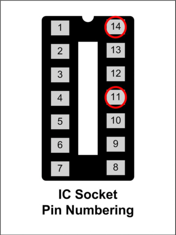
- Momentarily connect a jumper (small piece of wire) between U10 IC socket pin 13 and pin 14.
- Channel 2 LED should light-->This is the HB LED. Once again, the chip numbering is specific to the Renard 64XC. Some Renard boards have specific LEDs for the HB or "Heart Beat" Function.
- Momentarily connect a jumper between U10 IC socket pin 10 and pin 14
- Channel 5 LED should light -->This is the ZC or "Zero Crossing" LED.
- Momentarily connect a jumper between U10 IC socket pin 9 and pin 14
- Channel 6 LED should light -->This is the SD or "Data" LED.
- Momentarily connect a jumper between U10 IC socket pin 8 and pin 14
- Channel 7 LED should light -->This is the FE or "Framing Error" LED.
- Momentarily connect a jumper between U10 IC socket pin 7 and pin 14
- Channel 8 LED should light -->This is the OE or "Overun" LED.
- If any of the LEDs in steps 11 thru 15 did not light, then go to the Renard 64XC Troubleshooting Guide.
- Turn OFF AC power.
- Install a SSR like the SSRez into J12 with a known good straight through CAT5 cable. If you are not sure that the cable is good, use the DMM to ring out the cable.
- Attach some test lights to the SSR terminal block for Channel 1.
- Turn ON AC power.
- The power LED on the SSR should be on.
- Test lights should be OFF.
- Momentarily connect a jumper (small piece of wire) between U10 IC socket pin 3 and pin 14.
- Test lights should come ON when the jumper is connected.
- If either step 23 or step 24 failed, then go to the Renard 64XC Troubleshooting Guide.
- Repeat steps 18 thru 25 using the information in the table. Once again, the IC Chip numbering and the Jack numbering are for the Renard 64XC.
Board Channel IC Socket Number Output Jack Test Lights at SSR Channel Connect jumper between Channel 1 U10 J12 Channel 1 Channel 2 U10 J12 Channel 2 Channel 3 U10 J12 Channel 3 Channel 4 U10 J12 Channel 4 Channel 5 U10 J8 Channel 1 Channel 6 U10 J8 Channel 2 Channel 7 U10 J8 Channel 3 Channel 8 U10 J8 Channel 4 Channel 9 U9 J11 Channel 1 Channel 10 U9 J11 Channel 2 Channel 11 U9 J11 Channel 3 Channel 12 U9 J11 Channel 4 Channel 13 U9 J7 Channel 1 Channel 14 U9 J7 Channel 2 Channel 15 U9 J7 Channel 3 Channel 16 U9 J7 Channel 4 Channel 17 U8 J10 Channel 1 Channel 18 U8 J10 Channel 2 Channel 19 U8 J10 Channel 3 Channel 20 U8 J10 Channel 4 Channel 21 U8 J6 Channel 1 Channel 22 U8 J6 Channel 2 Channel 23 U8 J6 Channel 3 Channel 24 U8 J6 Channel 4 Channel 25 U7 J9 Channel 1 Channel 26 U7 J9 Channel 2 Channel 27 U7 J9 Channel 3 Channel 28 U7 J9 Channel 4 Channel 29 U7 J5 Channel 1 Channel 30 U7 J5 Channel 2 Channel 31 U7 J5 Channel 3 Channel 32 U7 J5 Channel 4 Channel 33 U14 J21 Channel 1 Channel 34 U14 J21 Channel 2 Channel 35 U14 J21 Channel 3 Channel 36 U14 J21 Channel 4 Channel 37 U14 J16 Channel 1 Channel 38 U14 J16 Channel 2 Channel 39 U14 J16 Channel 3 Channel 40 U14 J16 Channel 4 Channel 41 U13 J20 Channel 1 Channel 42 U13 J20 Channel 2 Channel 43 U13 J20 Channel 3 Channel 44 U13 J20 Channel 4 Channel 45 U13 J15 Channel 1 Channel 46 U13 J15 Channel 2 Channel 47 U13 J15 Channel 3 Channel 48 U13 J15 Channel 4 Channel 49 U12 J19 Channel 1 Channel 50 U12 J19 Channel 2 Channel 51 U12 J19 Channel 3 Channel 52 U12 J19 Channel 4 Channel 53 U12 J14 Channel 1 Channel 54 U12 J14 Channel 2 Channel 55 U12 J14 Channel 3 Channel 56 U12 J14 Channel 4 Channel 57 U11 J18 Channel 1 Channel 58 U11 J18 Channel 2 Channel 59 U11 J18 Channel 3 Channel 60 U11 J18 Channel 4 Channel 61 U11 J13 Channel 1 Channel 62 U11 J13 Channel 2 Channel 63 U11 J13 Channel 3 Channel 64 U11 J13 Channel 4
- Turn OFF AC power.
- Install optocoupler U2.
- Install two (2) RS232/RS485 Interface ICs U4 and U5.
- If you have a PIC programmed with the Renard Diagnostic Firmware continue with step 27.
- If you only have a PIC programmed with the Renard Operational Firmware then go to step 43.
- Install PIC microcontroller U10 programmed with the Renard Diagnostic Firmware.
- If desired, attach SSRs with lights to J12 and J8 with CAT5 Cable. The diagnostics can be done with only the on-board Channel LEDs.
- Turn ON AC power
NOTE:
The following step only applies if you are using the Beta Renard Diagnostic Firmware.
If you are using the proven/existing Renard Diagnostic Firmware just skip this step.
- The Renard Diagnostic Firmware should perform the following channel test:
- All channels ON for approx. 2 seconds.
- All channels OFF for approx. 2 seconds.
- Channel 1 LED and Channel 1 turns ON for approx. 1 second then turns OFF.
- Channel 2 LED and Channel 2 (HB LED) turns ON for approx. 1 second then turns OFF.
- Channel 3 LED and Channel 3 turns ON for approx. 1 second then turns OFF.
- Channel 4 LED and Channel 4 turns ON for approx. 1 second then turns OFF.
- Channel 5 LED and Channel 5 (ZC LED) turns ON for approx. 1 second then turns OFF.
- Channel 6 LED and Channel 6 (SD LED) turns ON for approx. 1 second then turns OFF.
- Channel 7 LED and Channel 7 (FE LED) turns ON for approx. 1 second then turns OFF.
- Channel 8 LED and Channel 8 (OE LED) turns ON for approx. 1 second then turns OFF.
- The above routine is done three times.
- The above routine is done three times.
- The Renard Diagnostic Firmware should now be blinking the HB LED (Channel 2) and ZC LED (Channel 5). All other channels/LEDs should be OFF.
- If either step 30 or step 31 failed, then go to the Renard 64XC Troubleshooting Guide.
- Turn OFF AC power.
- Connect a data cable to the computer running Vixen to either J4 or J22 on the Renard board..
- If receiving RS232 data from the computer place a shunt on JP1.
- Turn ON AC power.
- Wait for the diagnostics routine in steps 30/31 to complete.
REMINDER:
Make sure that Vixen is configured correctly before attempting the next step.
The settings for the Renard Dimmer Plug-In should be set as shown on
The Renard 64XC Controller Board wiki page. The only difference would be to
set the baud rate to 19200 for the non-beta Renard Diagnostic Firmware.
- Run a Vixen sequence.
NOTE:
Vixen only sends out data when there is a change in event data.
So make sure that the test sequence you are using has frequent changes in the event data..
- SD LED (Channel 6) will be ON whenever Vixen sends data to the Renard 64XC. The FE (Channel 7) and OE LEDs (Channel 8) should remain OFF.
- If incorrect , then go to the Renard 64XC Troubleshooting Guide
- Turn OFF AC power
- Remove U10
- To verify other functional PICs, repeat steps 27 thru 40 with the other seven (7) PICs
- Install PIC microcontrollers U7-U14 programmed with the Renard Operational Firmware.
- Turn ON AC power
REMINDER:
Make sure that Vixen is configured correctly before attempting the next step.
The settings for the Renard Dimmer Plug-In should be set as shown on
The Renard 64XC Controller Board wiki page.
- Run a Vixen sequence
- If the outputs do not respond correctly, then go to the Renard 64XC Troubleshooting Guide
