Renard8: Difference between revisions
Phil Short (talk | contribs) (New page: === First PCB Revision === This board can be distinguished by the letters XA on the solder side of the board, and by not having any silkscreen or soldermask. ==== Schematic ==== [[Image...) |
Phil Short (talk | contribs) (→BOM) |
||
| Line 22: | Line 22: | ||
==== BOM ==== | ==== BOM ==== | ||
Note: this BOM is slightly different from the previously published versions. The preferred part for diode D3 is now a BAT42 diode, because it has lower forward voltage drop and will fit in the holes on the board better. The old parts can continue to be used on previously assembled and working boards. | |||
<pre> | <pre> | ||
| Line 43: | Line 45: | ||
1 78-1N5229B 4.3v 0.5w Zener D2 | 1 78-1N5229B 4.3v 0.5w Zener D2 | ||
1 78-1N5239B 9.1v 0.5w Zener D1 | 1 78-1N5239B 9.1v 0.5w Zener D1 | ||
1 625-BAT42 | 1 625-BAT42 30V 100mA Schottky Diode D3 | ||
or (not preferred) | or (not preferred) | ||
1 625-1N5819-E3 50V 1A Schottky Diode D3 | 1 625-1N5819-E3 50V 1A Schottky Diode D3 | ||
Revision as of 16:18, 29 June 2007
First PCB Revision
This board can be distinguished by the letters XA on the solder side of the board, and by not having any silkscreen or soldermask.
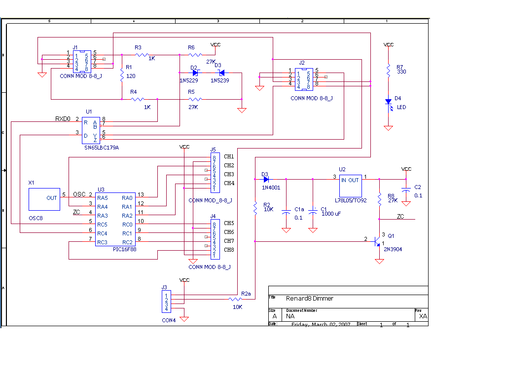
Schematic
This schematic is intended to exactly represent the first revision of the PCB. As such, the board has three known issues that will be changed on the next revision of the PCB (if there is one).
1) The order of the outputs on J4, J5 is exactly reversed from that of the Renard16, Renard64 and other Renard boards. Output 1 appears on the connector (J5, pin 8) where Output 8 would be expected (based on the other boards) instead of the expected location (J4, pin 2), and so forth. The power and ground connections are in the proper and expected location on these connectors.
2) The RS232/RS485 connections on pins 4,5 of J1 and J2 are transposed with respect to the other boards.
3) The input biasing resistors (R5, R6) are connected wrong, so that they force the serial input on the PIC to go low when the input cable to the board is disconnected. This does not appear to cause any problems at the time.
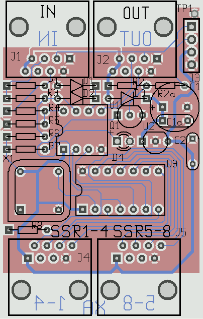
PCB Image
The blue layer is the solder side, and the red layer represents the component side. The silkscreen layer is shown on this composite image to indicate where the various components are located. None of the boards manufactured to date actually include the silkscreen or soldermask layers.
BOM
Note: this BOM is slightly different from the previously published versions. The preferred part for diode D3 is now a BAT42 diode, because it has lower forward voltage drop and will fit in the holes on the board better. The old parts can continue to be used on previously assembled and working boards.
PCB
1  TBA                   Renard8 PCB

Resistors

3  299-27K-RC            27K Resistor, 1/4 W, Axial                       R5, R6, R8
2  299-1K-RC              1K Resistor, 1/4 W, Axial                       R3, R4
1  660-MF1/4DCT52R1200F  120 Resistor, 1/4 W, Axial                       R1
1  299-330-RC            330 Resistor, 1/4 W, Axial                       R7
1  299-10K-RC            10K Resistor, 1/4 W, Axial                       R2

Capacitors

1 80-C322C104K5R         0.1 uF Radial-lead Ceramic Capacitor             C2
1 140-XRL16V1000-RC      1000 uF, 16V Electrolytic Capacitor              C1

Diodes
1  78-1N5229B            4.3v 0.5w Zener                                  D2
1  78-1N5239B            9.1v 0.5w Zener                                  D1
1  625-BAT42             30V 100mA Schottky Diode                         D3
                             or (not preferred)
1  625-1N5819-E3         50V 1A Schottky Diode                            D3
                             or (not preferred)
1  625-1N4001-E3         50v 1A Diode                                     D3
1  604-WP7104GT          T1 Green LED                                     D4

Transistors
1  512-2N3904TA          Small Signal Transistor                          Q1

Connectors

4  571-5202514           AMP Modular Jacks, Right Angle                   J1, J2, J4, J5
         or
4  571-5564161           AMP Modular Jacks, Top Entry
         or
4  538-95003-2881        Molex Modular Jacks, Vertical PCB mount
1  575-199314            14 Pin Low Profile IC Socket                     XU3

ICs

1  595-SN65LBC179PE4     RS485 Receiver/Transmitter 65LBC179              U1
1  579-PIC16F688-I/P     PIC16F688, unprogrammed, DIP14, Industrial Temp  U3
1  595-UA78L05ACLPRE3    Regulator, 5V                                    U2
If you can obtain it, a LP2950-5.0 regulator is preferred for U2 in place of the 78L05, because it has a lower dropout voltage and lower quiescent current.
Second Revision
TBA

