Ren-W Troubleshooting: Difference between revisions
Jump to navigation
Jump to search
Dirknerkle (talk | contribs) No edit summary |
Dirknerkle (talk | contribs) No edit summary |
||
| Line 15: | Line 15: | ||
[[File:Ren-w-bottom-view.GIF |400px]] | |||
*When you study the underside (copper) side of the circuit board, a few things become apparent: | *When you study the underside (copper) side of the circuit board, a few things become apparent: | ||
Revision as of 05:05, 3 February 2010
The Ren-W circuit board is a very simple design but good soldering technique is still extremely important.
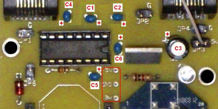
Voltage Measurements: three test points are just below pin 16 of the MAX232 chip/socket:
- Be certain that the following components are mounted on the board properly:
- The notch on the MAX232 chip faces to the right, toward the U1 voltage regulator.
- The zener diode (D1) has the black stripe on the TOP, next to the JP6 header pins.
- The 3.3 voltage regulator (U1) has the metal tab facing up, toward the JP2 header pins.
- The electrolytic capacitor (C3) has the - stripe facing DOWN toward the LED, which means the + side is up toward the J2 jack.
- The LED (D2) while not shown in this photo, has the cathode (flat side) facing the mounting hole to its right.
- Resistor R1 (33 ohms) is immediately below the MAX232 chip. The resistor has no polarity concerns.
- Resistor R2 (1k ohms) is immediately to the left of the LED. The resistor has no polarity concerns.
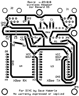
- When you study the underside (copper) side of the circuit board, a few things become apparent:

