Ren-W BOM and Construction
Master Parts List (with Ren-W Part# and Mouser Part#)
- Qty -- Description (Ren-W Part)
- 1 or 2 -- RJ45 jacks, side or top entry (J1, J2) Mouser# 571-5520251-4 (side entry) 571-5556416-1 (top entry)
- 6 -- 2-pin vertical PCB headers (JP1-JP6) Mouser# 538-22-03-2021 (fewer may be necessary – see note below)
- 5 -- 1 uf capacitors (non-polarized - C1, C2, C4, C5, C6) Mouser# 810-FK24Y5V1H105Z (Note: 1 uf 16v electrolytic capacitors may be substituted if you wish; polarity markings are provided on the board as a convenience if you use electrolytics.)
- 1 -- 100uf, 16v electrolytic capacitor (C3) Mouser# 647-UVR1C101MDD
- 1 -- 3.3v 1w zener diode (D1) Mouser# 583-1N4728A-B
- 1 -- 33 ohm ¼w resistor (R1) Mouser# 291-33-RC (299-33-RC 1/8 watt is also okay)
- 1 -- 1k ohm ¼w resistor (optional) (R2) Mouser# 291-1K-RC (299-1K-RC 1/8 watt is also okay)
- 1 -- LED (any color – optional) (D2) Mouser# 604-WP7104GT (green transparent)
- 1 -- 16-pin DIP socket (optional) Mouser# 571-1-390261-4
- 1 -- 3.3v positive voltage regulator (U1) Mouser# 595-UA78M33CKCSE3
- 1 -- RS-232 Interface ICs Dual EIA-232 Driver Mouser# 595-MAX232N
- 1 -- XBee Wireless RF modules (Pro version w/1" whip antenna is Mouser# 888-XBP24-AWI-001. The SMA version is #888-XBP24-ASI-001)
- 2 -- Female SL Connectors (optional) Mouser# 538-16-02-0102
- 1 -- Ren-W circuit board (etch your own in the true DIYC spirit, or contact dirknerkle for pre-made boards)
- 2/4 -- 2mm x 10-pin XBee female headers (H1-H4) Mouser# M22-7131042 or also available from SparkFun Electronics as part# PRT-08272 ($1 each)
- 1 -- Ren-C users: Snap Choke Core Balun - Radio Shack part# 273-0069
- Rev6 board BOM Differences
- The only difference is the Rev6 board needs only one RJ45 jack and only two XBee female headers. Otherwise, parts are the same.
- Here's a direct link to the complete Mouser BOM: Ren-W BOM
- Here's a direct link to the Express PCB source file for the STANDARD board: Ren-W STD PCB file
- Here's a direct link to the Express PCB source file for the SMA board: Ren-W SMA PCB file
- Here's a direct link to the schematic for the Ren-W board: Ren-W_Schematic.JPG file
- Go to www.expresspcb.com to download their free PCB software to open the PCB file.
PCB Parts Layout
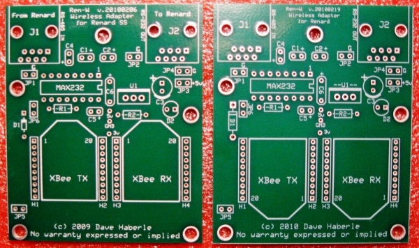
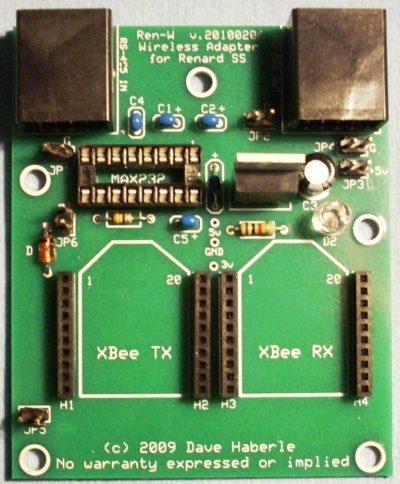
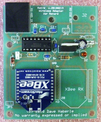
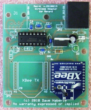
- The only important difference between the standard board and the SMA board is the orientation of the XBee modules. The standard board has the modules pointing upward; the SMA version has them pointing downward to allow for the long RPSMA antenna connector. Pay careful attention to the orientation of the XBee when plugging it into the board. If you have the standard board, plugging in an XBee module with an SMA connector upside-down will NOT WORK. Likewise, plugging in an XBee with a 1" whip the wrong way on an SMA board won't work, either.
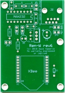
- The latest Rev6 version of the board has space for only one XBee module and uses a jumper to make the board be either a transmitter (TX) or receiver (RX). The Rev6 board cannot function as a repeater board as it has only one RJ45 jack, but it is about 30% smaller in size and has fewer parts so it's slightly less expensive to build.
Construction Step-by-step
- The construction steps are identical for both the standard and SMA version of the board, and the Rev6 board uses the same part numbers. Caution - the pins on these headers are quite tiny and require very little solder. Too much solder may flow down and fill the pin hole in the header itself and prevent plugging in the XBee later on.
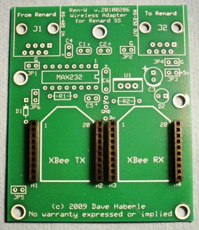
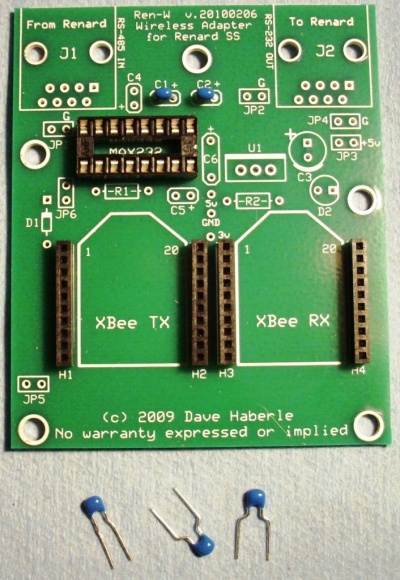
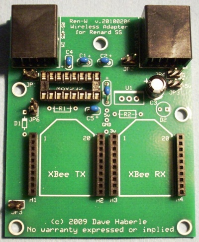
- 1. Solder 2mm female headers at locations H1, H2, H3, H4 or:
- TX only: only H1, H2 are required
- RX only: only H3, H4 are required
- E-mode repeater: only H1, H2 are required.
- Normal repeater mode: all four headers required
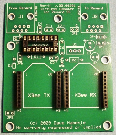
- 2. Solder the 16-pin DIP socket into the MAX232 location. Note the position of pin 1; the notch faces to the right. If no socket is to be used, solder the MAX232 directly to the Ren-W board; verify the pin orientation before soldering.
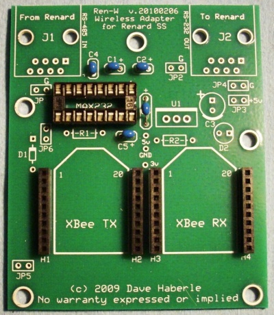
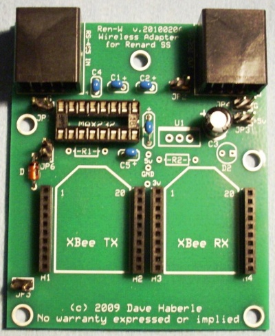
- 3. Solder capacitors C1 and C2. You may wish to straighten the leads to fit the holes better such as the example at the bottom of the picture. There are no polarity concerns for non-polarized capacitors. (Note: The polarity markings on the board are for the convenience of users who are using electrolytic capacitors instead of the non-polarized type.
- 4. OPTIONAL: Solder non-polarized capacitors C4, C5 and C6. Like C1 and C2, if electrolytic capacitors are used, observe the + polarity markings on the board. (Note: C4, C5 and C6 do a lot to clean up the RS-232 signal the Ren-W provides to the Renard controller, and these are essential if connecting the Ren-W to a Ren-C/595 or Ren-C/Grinch. However, in testing, C4, C5 and C6 were proven to be unnecessary when using the Ren-W with Renard SS controllers.)
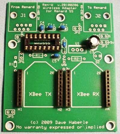
- 5. Solder electrolytic capacitor C3. Note the polarity: the + side into the square pad (top) closer to jack J2 which means the stripe on the capacitor faces DOWN.
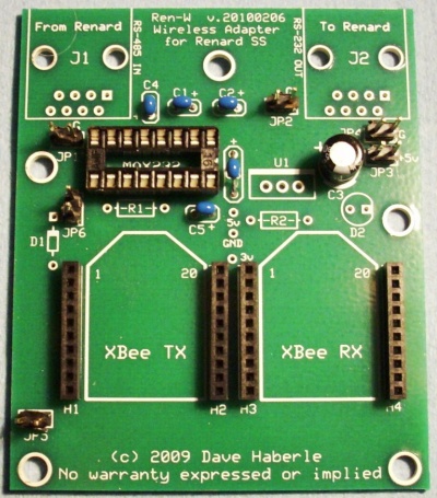
- 6. Solder 2-pin headers JP1, JP2, JP3, JP4, JP5, JP6. (Note: JP1 and JP2 are optional.) The header pins are a tight fit; be careful as you wiggle them into their respective holes.
- 7. Solder RJ45 jacks J1, J2
- TX only: only J1 is required
- RX only: only J2 is required
- Normal repeater and E-mode repeater: both J1 and J2 are required
- 8. Solder zener diode D1. Note the polarity – the band on the diode must be facing up, next to header JP6.
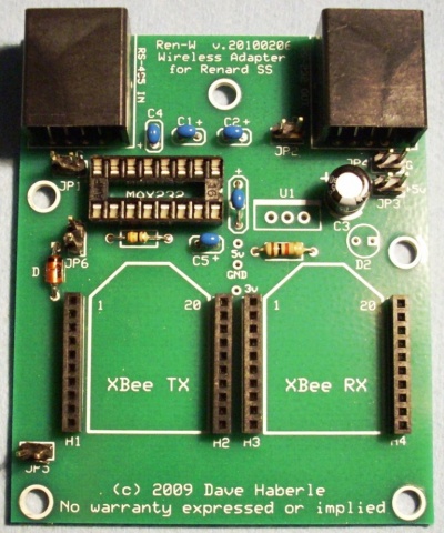
- 9. Solder resistors R1 (orange-orange-black) and R2 (brown-black-red). R2 is only required if the optional power LED (D2) is used. No polarity concerns.
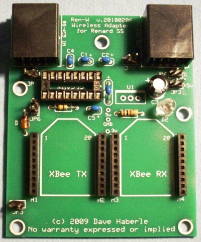
- 10. Solder the optional power LED at position D2. Note the polarity – the flat side/cathode/shorter lead faces to the mounting hole immediately to the right of D2.
- 11. Solder the 3.3v voltage regulator U1. The heat sink side faces toward JP2 (top). The need for an additional heat sink is highly unlikely as the supply voltage is only 5vdc. At this point, applying power to the board should light the LED (if installed) and the voltage test points in the middle of the board should register the proper voltages. Disconnect power before continuing with the next step.
- 12. Install the MAX232 and XBee module(s) in their respective sockets: use the XBee RX side for a receive-only board, the XBee TX side for a transmit-only board. Note the position of pin 1.
- 13. Install optional jumper shunt at JP6 if necessary. This bypasses the R1 resistor (33 ohms) and allows a weaker RS-485 signal through to the XBee radio in transmit mode. Normally, this jumper shunt is not necessary.
- 14. Install optional jumper shunt at JP5 if necessary. This makes the Ren-W into an E-Mode repeater where a single XBee module in the TX position serves as both the receiver and transmitter.
- 15. CAUTION: Never place jumper shunts across JP1 or JP2!
- 16. CAUTION: Never place jumper shunts across either pin of JP3 to either pin of JP4!
- 17. REV-6 board only: install 2-pin jumper headers at the TX and RX locations.
Powering the Ren-W board
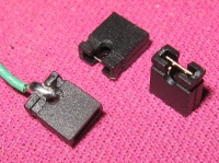
- A nifty solution that retains the SS controller’s ability to use the diagnostic LEDs is to solder each end of a single strand of cat5 wire to an open jumper shunt such as the photo above. Alternately, you may wish to make your own power cable using two female SL connectors; use a small piece of shrink tubing around the connector for insulation safety. (Both pins on the Ren-W’s JP3 header are +5vdc; both JP4 pins are ground connections.)
- With WayneJ's SS line of boards, the Ren-W draws its +5vdc power from the left pin of the board’s JP3 header (photo above); the ground power connection is made when the Ren-W is connected to either of the SS controller's RJ45 jacks. If you used the open jumper shunts to make your cable, simply plug the shunts into the JP3 headers on both the SS controller and the Ren-W.
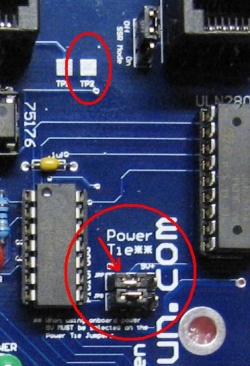
- With Frank Kostyun's Ren24 ver 3.3, +5vdc can be taken at TP2 (test point 2). You may drill a small hole in the pad if you wish to solder-in a single pin header. With the Ren24LV the red circles show places where 5vdc can be found: TP2 and the "Power Tie" (both circled in red in the above photo). The power tie includes six places for jumper header pins, the TOP LEFT of which carries +5vdc (red arrow) Remember, ground is made automatically when the cat5 cable is plugged in.
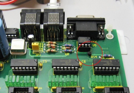
- With Wjohn's Ren64 (version XC5) there is a small, unmarked +5vdc test point immediately below pin 8 of U5 (the rightmost ST485BN chip) and just left of R14. Solder-in a single header pin if you like such as the example above (red circle).
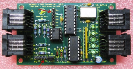
- With Wjohn's Ren-C, +5vdc can be taken from the header pin immediately to the left of the Q1 transistor. The pin is marked VCC. Another +5vd VCC location is the 2nd from the top pin of the 6-pin JP6 programming header. Either location is fine. Both are marked with red arrows in the photo above.
Connecting the Ren-W to a Renard SS Controller
- Connect JP3 to JP3 on the SS to power the Ren-W (5vdc).
- Ren-W as a transmit only node: connect only J1 to J1 on the SS. Leave J2 on the Ren-W unconnected.
- Ren-W as a receive only node: connect only J2 to J2 on the SS. Leave J1 on the Ren-W unconnected.
- Ren-W as a standard repeater: connect J1 to J1 and J2 to J2 on the SS. (A standard repeater has TWO XBee modules.)
- Ren-W as an E-mode repeater: connect J1 to J1 and J2 to J2 on the SS, add a jumper on the Ren-W’s JP5 and make sure the Ren-W has only a single XBee module plugged into the TX (left) position. (An E-Mode repeater has only ONE XBee module.)
- On the SS controller, be sure JP1 is jumpered to accept RS-232 communication and jumper JP2 as well.
- If connecting to the RS-IN of a Ren-C, be sure to affix a snap choke core balun on the cat5 cable (Radio Shack part# 273-0069).
- Rev6 board only: since this board has only one RJ45 jack, it can be plugged into either the J1 or J2 jack on the Renard controller. If using the Rev6 as a receiver, place a jumper shunt on the RX header and connect J2 to the RS INPUT jack of the controller. If using the Rev6 as a receiver, place a jumper shunt on the TX header and connect J2 to the RS OUTPUT jack of the controller. Note that the Rev6 board cannot be used as a "repeater" board which both receives and retransmits out. However, it can be used to transmit from a wired Renard controller to another Ren-W. Of course, a Rev6 can also be a main transmitter board at the PC as well.
What are JP1, JP2 and JP6 used for?
- JP1 is an optional RS-485 input connection. Because an XBee module can be programmed via serial communications using a simple AT commands from within a terminal program such as Windows Hyperterminal, these headers provide external access to the R1IN (pin 13, JP1) and T1OUT (pin 14, JP2) serial connections of the MAX232 chip, which in turn, communicates with the XBee module. Both data and ground are provided; ground is the right pin and is marked with G. Using the XCTU software and an XBee programmer board is vastly more convenient that manually configuring a module using AT commands but Digi provides ample documentation for AT command line programming. You can also measure the input voltage of the RS-485 signal at JP1; an acceptable range is +3.3 to +4.8 vdc. It is not expected that this voltage will exceed 5vdc.
- JP2 is an optional RS-232 output connection and can also be used to connect Ren-W to other serial devices. The output voltage is inverted and should be -5.0 to -5.5vdc, depending on the original input voltage.
- Caution: never place a shunt jumper across JP1 or JP2, or across either pin of JP3 to either pin of JP4.
- JP6 is used to bypass the 33ohm resistor R1 which helps moderate the RS-485 serial signal’s current. The combination of R1 and zener diode D1 form a voltage/current protection circuit that limits the serial voltage to a maximum of 3.3 volts before it enters the XBee module’s DIN port. However, not all RS-485 serial signals are of the same voltage and if your serial signal is less than +3.3 volts, you may find that the integrity of transmitted data may increase by placing a shunt jumper on JP6 to bypass resistor R1. If the serial signal is +3.8 vdc or greater, you should leave JP6 open. The XBee module includes a modicum of internal protection and in testing, we found that an XBee can accommodate +5vdc at the input DIN for a short period of time (a few seconds), after which the XBee may stop responding and appear to “lock up.” Temporarily removing power to the board usually resets the XBee so that it will function again.
Other Voltage Test Points
- Almost in the exact center of the Ren-W board are three test points marked 5vdc, GND and 3vdc (actually 3.3v). While the actual voltages may vary slightly, the tested values should be very close to those figures. Our prototype measured 4.96v and 3.29v.
Economy Ren-W Construction
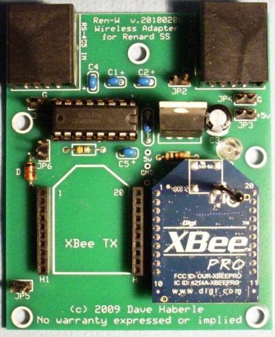
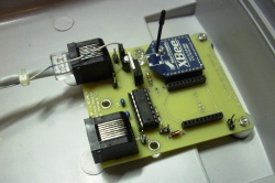
- If you know exactly how many receive-only and/or transmit-only boards you need and want to save some cash, you can economize by not populating the board with parts that will not be used. For example, below are pictures of stripped-down yet fully functional transmit-only (left) and receive-only (right) boards. Note the parts that are missing on each board. These examples also show the standard XBee radio, not the Pro version, which cuts cost even more, although the standard XBee is quite limited in transmission range. (Price comparison: the Standard Xbee is $19, XBee Pro is $32, XBee Pro with SMA connector is $34.):
- Bottom line: a fully-populated Ren-W board totals about $43.38 for parts with the XBee Pro radio. If you don't need the extra power of the Pro version and opt for the standard XBee, you could build a transmit-only or receive-only board for about $26. Home-etch the boards yourself and you could have a fully-functional two-station system for about $50, and using the XBee Pro version would cost only $26 more for the pair. So if you're on the fence about wireless, you can see that it doesn't have to cost an arm-and-a-leg.
Mounting a Ren-W and SS24 Controller in a CG2000 Enclosure
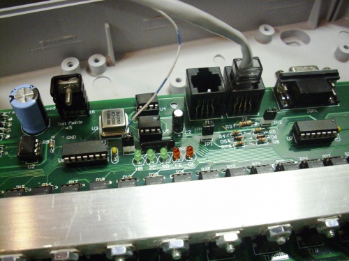
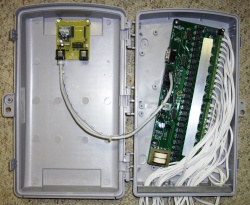
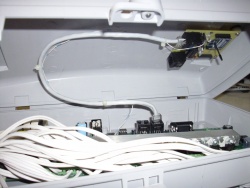
Using side-entry RJ45s on the Ren-W and looping a cat5 cable from the Ren-W to the SS24, stress is minimized on all RJ45 connectors and the case can easily be fully opened. The Ren-W is mounted at the top of the case, to minimize magnetic interference from the SS24's transformer, and the SS24 is mounted diagonally in the CG2000 case to allow room for the antenna as well as a little additional distance from the triacs, another potential source of interference.
Additional Ren-W Links
